Specification
| T5L2 ASIC |
Designed by DWIN. Mass production in 2019, 1MBytes Nor Flash on the chip, 512KBytes used to store the user database. Rewrite cycle: over 100,000 times | |
| Color | 16.7M(16777216) | |
| Resolution | 1024×768 | |
| Backlight | LED | |
| Brightness | 250nit | |
| Panel Type | IPS | |
| Viewing Angle | 85/85/85/85 (L/R/U/D) | |
| Active Area (A.A.) | 162.00mm(W)×121.50mm(H) | |
| View Area(V.A) | 162.60mm (W)×122.20mm (H) | |
| Power Voltage | 6~36V,Typ. 12V | |
| Operation Current | VCC = +12V, Backlight on,255mA | |
| VCC = +12V, Backlight off, 105mA | ||
| Working Temperature | -20~70℃ | |
| Storage Temperature | -30~85℃ | |
| Working Humidity | 10%~90%RH | |
| Socket | 50Pin-0.5mm FCC | |
| SD slot | YES (SDHC/FAT32 Format) | |
| USB interface | YES | |
| Flash | Space of Font: 4-28Mbytes | |
| Picture Storage:28-4Mbytes | ||
| RAM | 128Kbytes | |
| Nor Flash | 512Kbytes | |
| EKT080A | Capacitance touch panel, buzzer | |
| Dimension | 199.39mm(W) ×148.84mm(H) ×21.90mm(T) | |
| Net Weight | 410g | |
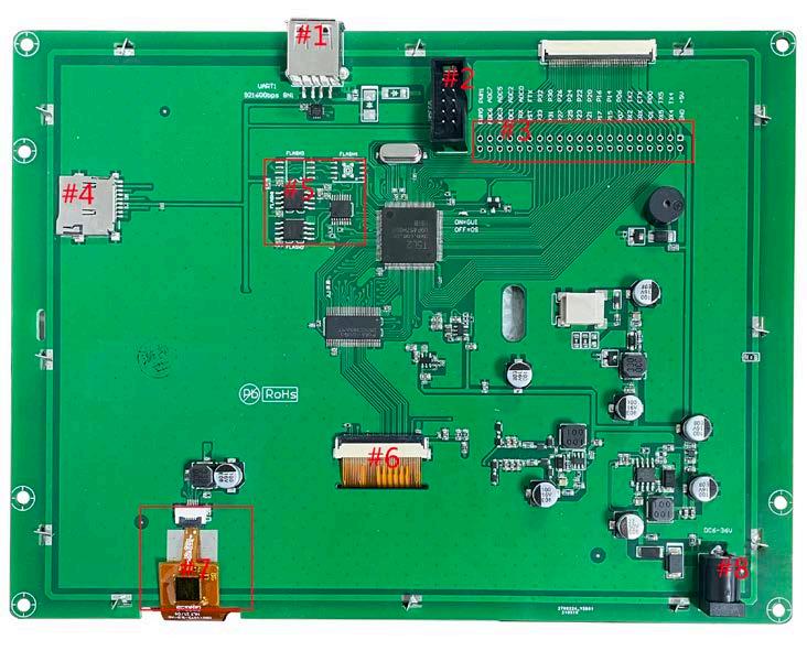
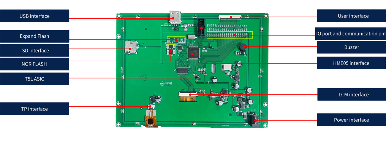
| 1# | USB interface, uart1 can be selected | |
| 2# | JTAG interface, connected to hme05 emulator or pgt05 burner, used to burn the underlying kernel firmware | |
| 3# | 2.54mm through hole pad GUI / OS CPU outgoing interface | |
| 4# | SD card burning interface | |
| 5# | Flash expansion module can expand 2 Flash modules | |
| 6# | LCD interface | |
| 7# | Capacitive touch screen interface | |
| 8# | 6-36V wide voltage power supply interface | |
| PIN | Definition | Description |
| 1# | GND | Common ground |
| 2# | RX4 | UART4 Data reception |
| 3# | RX5 | UART5 Data reception |
| 4# | P01 | I / O mouth |
| 5# | CRX | CAN interface data reception |
| 6# | RX2 | UART2 data receiving |
| 7# | P07 | I / O |
| 8# | P15 | I / O |
| 9# | P17 | I / O |
| 10# | P21 | I / O |
| 11# | P23 | I / O |
| 12# | P25 | I / O |
| 13# | P27 | I / O |
| 14# | P31 | I / O |
| 15# | P33 | I / O |
| 16# | FTX | FSK transceiver data reception |
| 17# | ADC0 | AD input |
| 18# | ADC2 | AD input |
| 19# | ADC5 | AD input |
| 20# | ADC7 | AD input |
| 21# | PWM1 | 16bit PWM output |
| 22# | 5V | power input |
| 23# | TX4 | UART4 data transmission |
| 24# | TX5 | UART5 data transmission |
| 25# | P0.0 | I / O |
| 26# | CTX | CAN interface data transmission |
| 27# | TX2 | UART2 data transmission |
| 28# | P06 | I / O |
| 29# | P14 | I / O |
| 30# | P16 | I / O |
| 31# | P20 | I / O |
| 32# | P22 | I / O |
| 33# | P24 | I / O |
| 34# | P26 | I / O |
| 35# | P30 | I / O |
| 36# | P32 | I / O |
| 37# | RSTN | System reset input |
| 38# | FRX | FSK transceiver data transmission |
| 39# | ADC1 | AD input |
| 40# | ADC3 | AD input |
| 41# | ADC6 | AD input |
| 42# | PWM0 | 16bit PWM output |

Model: EKT080A