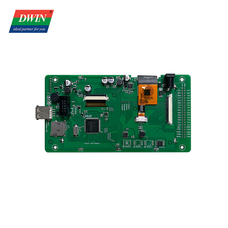
Specification
| T5L0 ASIC | DWIN T5L0 LCD drive IC was published in 2020, 1MBytes Nor Flash on the chip, 512KBytes used to store the user database. | |
| Color | 262K(262144)colors | |
| LCD Type | TN, TFT LCD | |
| Viewing Angle | Nomal viewing angle, 70/70/50/70(L/R/U/D) | |
| Display Area(A.A) | 108.00mm (W)×64.80mm (H) | |
| Resolution | 800×480 Pixel | |
| Backlight | LED | |
| Brightness | EKT050A: 250nit | |
| Power Voltage | 6~36V | |
| Operation Current | VCC = +12V, Backlight on,150mA | |
| VCC = +12V, Backlight off,90mA | ||
| Working Temperature | -20~70℃ | |
| Storage Temperature | -30~85℃ | |
| Working Humidity | 10%~90%RH | |
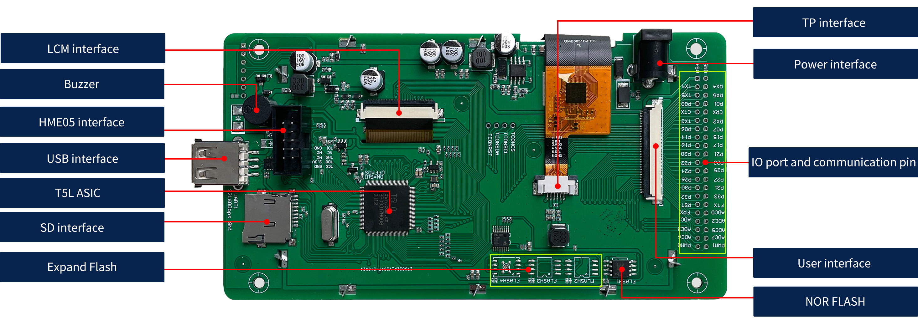
| Socket | 50Pin-0.5mm FCC | |
| USB Slot | Yes | |
| SD Slot | YES (SDHC/FAT32 Format) | |
| Flash | Space of Font: 4-12Mbytes | |
| Picture Storage:12-4Mbytes | ||
| RAM | 128Kbytes | |
| Nor Flash | 512Kbytes | |
| UI Version | TA / DGUSⅡ (DGUSⅡ pre-installed) | |
| Peripheral | Capacitive touch panel, Buzzer | |
| Dimension | 154.60mm (W) ×80.9mm (H) ×21.1mm(T) | |
| Net Weight | 160g | |
| PIN | Definition | Description |
| 1# | GND | Common ground |
| 2# | RX4 | UART4 Data reception |
| 3# | RX5 | UART5 Data reception |
| 4# | P01 | I / O mouth |
| 5# | CRX | CAN interface data reception |
| 6# | RX2 | UART2 data receiving |
| 7# | P07 | I / O |
| 8# | P15 | I / O |
| 9# | P17 | I / O |
| 10# | P21 | I / O |
| 11# | P23 | I / O |
| 12# | P25 | I / O |
| 13# | P27 | I / O |
| 14# | P31 | I / O |
| 15# | P33 | I / O |
| 16# | FTX | FSK transceiver data reception |
| 17# | ADC0 | AD input |
| 18# | ADC2 | AD input |
| 19# | ADC5 | AD input |
| 20# | ADC7 | AD input |
| 21# | PWM1 | 16bit PWM output |
| 22# | 5V | power input |
| 23# | TX4 | UART4 data transmission |
| 24# | TX5 | UART5 data transmission |
| 25# | P0.0 | I / O |
| 26# | CTX | CAN interface data transmission |
| 27# | TX2 | UART2 data transmission |
| 28# | P06 | I / O |
| 29# | P14 | I / O |
| 30# | P16 | I / O |
| 31# | P20 | I / O |
| 32# | P22 | I / O |
| 33# | P24 | I / O |
| 34# | P26 | I / O |
| 35# | P30 | I / O |
| 36# | P32 | I / O |
| 37# | RSTN | System reset input |
| 38# | FRX | FSK transceiver data transmission |
| 39# | ADC1 | AD input |
| 40# | ADC3 | AD input |
| 41# | ADC6 | AD input |
| 42# | PWM0 | 16bit PWM output |

DMG48270C043_03W (Commercial grade)