Specification
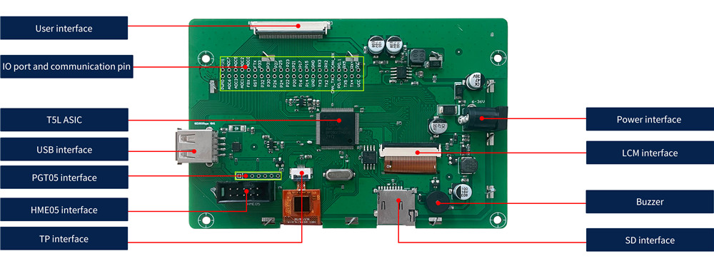
| T5L ASIC | DWIN self-designed 8051 LCD drive chip. Mass production in 2019, 1MBytes Nor Flash on the chip, 512KBytes used to store the user database. Rewrite cycle: over 100,000 times | |
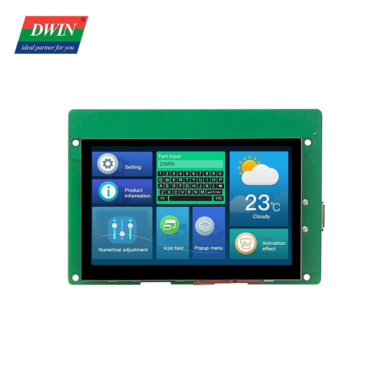
| Color | 262K (262144) colors | |
| Display Area(A.A) | 95.04mm(W)×53.86mm(H) | |
| Resolution | 480X272 Pixel | |
| Backlight | LED | |
| Brightness | EKT043C: 250nit 100 levels adjustment.(It's not recommend to set brightness to 1%~30% of the maximum, which may lead a flicker) | |
| LED Lifetime | ≥20000H(Continuous working with maximum brightness, time of the brightness decays to 50%) | |
| Type | Capacitive Touch | |
| Structure | G+G structure with surface cover of Asahi tempered glass | |
| Touch Mode | Support point touch and drag | |
| Surface Hardness | 6H | |
| Light Transmittance | Over 90% | |
| Life | Over 1,000,000 times touch | |
| Power Voltage | 6~36V | |
| Operation Current | VCC = +12V, Backlight on, 100mA | |
| VCC = +12V, Backlight off, 40mA | ||
| Working Temperature | -20~70℃(Typical 25℃) | |
| Storage Temperature | -30~85℃(Typical 25℃) | |
| Working Humidity | 10%~90%RH(Typical 25℃) | |
| Baudrate | 3150~3225600bps | |
| Output Voltage | Output 1, Iout = 1mA;3.0~3.3 V | |
| Output 0, Iout =-1mA;0~0.3 V | ||
| Input Voltage (RXD) |
Input 1, Iin = 1mA;2.4~5.0V | |
| Input 0, Iin = -1mA;0~0.5V | ||
| Interface | UART1: TTL | |
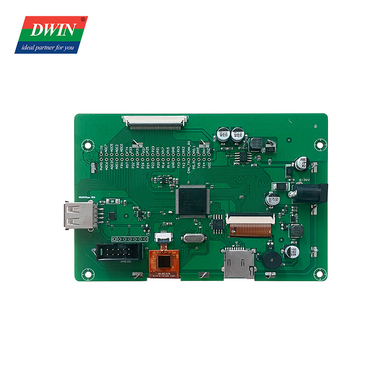
| Socket | 50Pin-0.5mm FCC, | |
| SD slot | YES (SDHC/FAT32 Format) | |
| Source opened for users | 20 I/Os, 3 UART, 1 CAN, 7 ADs, 2 PWMs | |
| Flash | Space of Font: 4-12Mbytes | |
| Picture Storage:12-4Mbytes | ||
| RAM | 128Kbytes | |
| Nor Flash | 512Kbytes | |
| UI Version | TA / DGUSⅡ (DGUSⅡ pre-installed) | |
| Peripheral | Capacitive touch panel, Buzzer | |
| Dimension | 125.22mm(W) ×85.80mm(H) ×19.40mm(T) | |
| Net Weight | 125g | |
| 1# | 2.54mm through-hole pad, GUI/OS CPU lead-out interface, silk prints on the other side | |
| 2# | USB interface, UART1 can be selected | |
| 3# | JTAG interface, connect to HME05 emulator, or connect to PGT05 burner to burn the underlying core firmware. | |
| 4# | 6-36V wide voltage power supply interface | |
| 5# | SD card burning interface | |
| PIN | Definition | Description |
| 1# | GND | Common ground |
| 2# | RX4 | UART4 Data reception |
| 3# | RX5 | UART5 Data reception |
| 4# | P01 | I / O mouth |
| 5# | CRX | CAN interface data reception |
| 6# | RX2 | UART2 data receiving |
| 7# | P07 | I / O |
| 8# | P15 | I / O |
| 9# | P17 | I / O |
| 10# | P21 | I / O |
| 11# | P23 | I / O |
| 12# | P25 | I / O |
| 13# | P27 | I / O |
| 14# | P31 | I / O |
| 15# | P33 | I / O |
| 16# | FTX | FSK transceiver data reception |
| 17# | ADC0 | AD input |
| 18# | ADC2 | AD input |
| 19# | ADC5 | AD input |
| 20# | ADC7 | AD input |
| 21# | PWM1 | 16bit PWM output |
| 22# | 5V | power input |
| 23# | TX4 | UART4 data transmission |
| 24# | TX5 | UART5 data transmission |
| 25# | P0.0 | I / O |
| 26# | CTX | CAN interface data transmission |
| 27# | TX2 | UART2 data transmission |
| 28# | P06 | I / O |
| 29# | P14 | I / O |
| 30# | P16 | I / O |
| 31# | P20 | I / O |
| 32# | P22 | I / O |
| 33# | P24 | I / O |
| 34# | P26 | I / O |
| 35# | P30 | I / O |
| 36# | P32 | I / O |
| 37# | RSTN | System reset input |
| 38# | FRX | FSK transceiver data transmission |
| 39# | ADC1 | AD input |
| 40# | ADC3 | AD input |
| 41# | ADC6 | AD input |
| 42# | PWM0 | 16bit PWM output |

EKT043B
Model: EKT070A