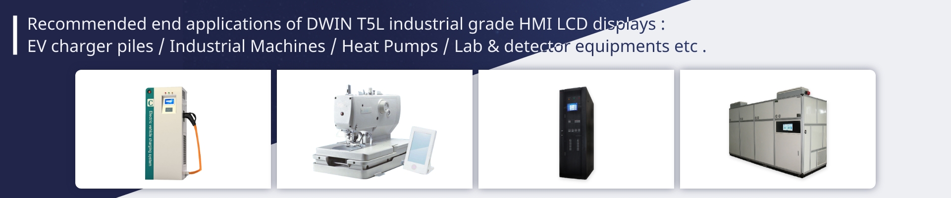

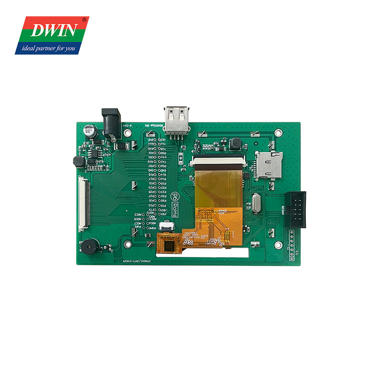
Specification
| T5L ASIC | Designed by DWIN. Mass production in 2019, 1MBytes Nor Flash on the chip, 512KBytes used to store the user database. Rewrite cycle: over 100,000 times | |
| Color | 262K(262144)colors | |
| LCD Type | IPS | |
| Viewing Angle | Wide viewing angle, 85°/85°/85°/85° (L/R/U/D) | |
| Display Area(A.A) | 70.08mm (W)×52.56mm (H) | |
| Resolution | 320×240 Pixel | |
| Backlight | LED | |
| Brightness | EKT035A: 270nit 100 levels adjustment.(It's not recommend to set brightness to 1%~30% of the maximum, which may lead a flicker) |
|
| LED Lifetime | ≥20000H(Continuous working with maximum brightness, time of the brightness decays to 50%) | |
| Power Voltage | 6~36V | |
| Operation Current | VCC = +12V, Backlight on,90mA | |
| VCC = +12V, Backlight off,30mA | ||
| Working Temperature | -20~70℃ (Typical 25℃) | |
| Storage Temperature | -30~85℃ (Typical 25℃) | |
| Working Humidity | 10%~90%RH (Typical 25℃) | |
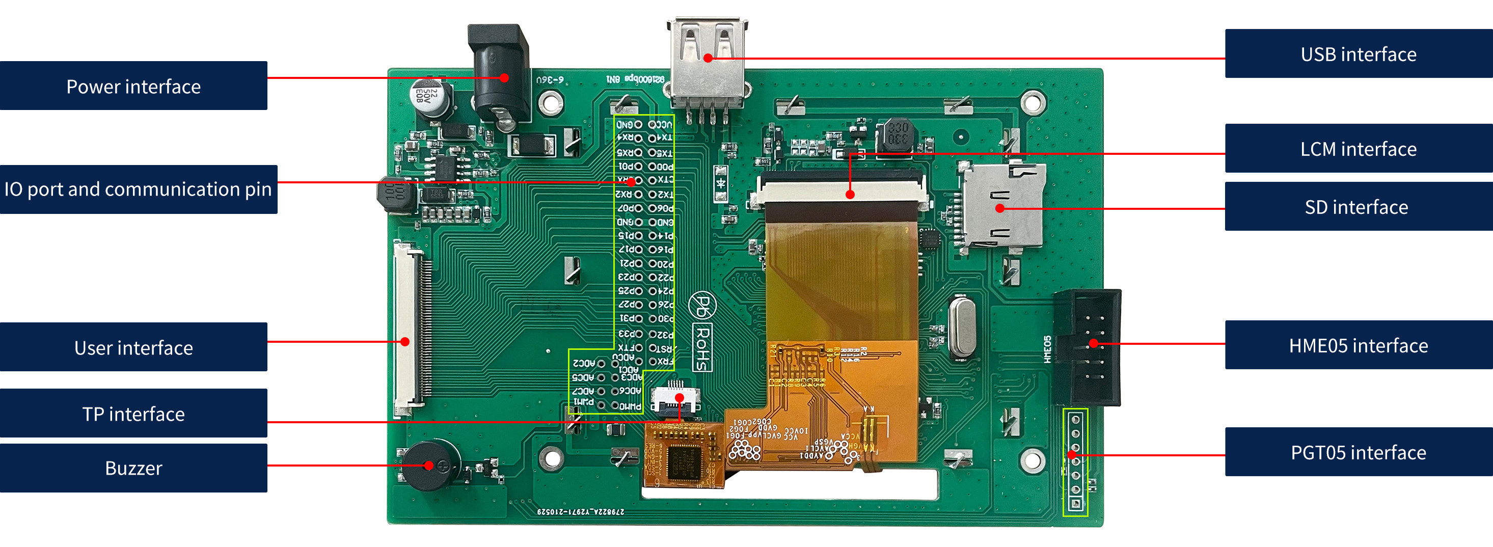
| Socket | 50Pin-0.5mm FCC | |
| USB | YES | |
| SD slot | YES (SDHC/FAT32 Format) | |
| Flash | Space of Font: 4-12Mbytes | |
| Picture Storage:12-4Mbytes | ||
| RAM | 128Kbytes | |
| Nor Flash | 512Kbytes | |
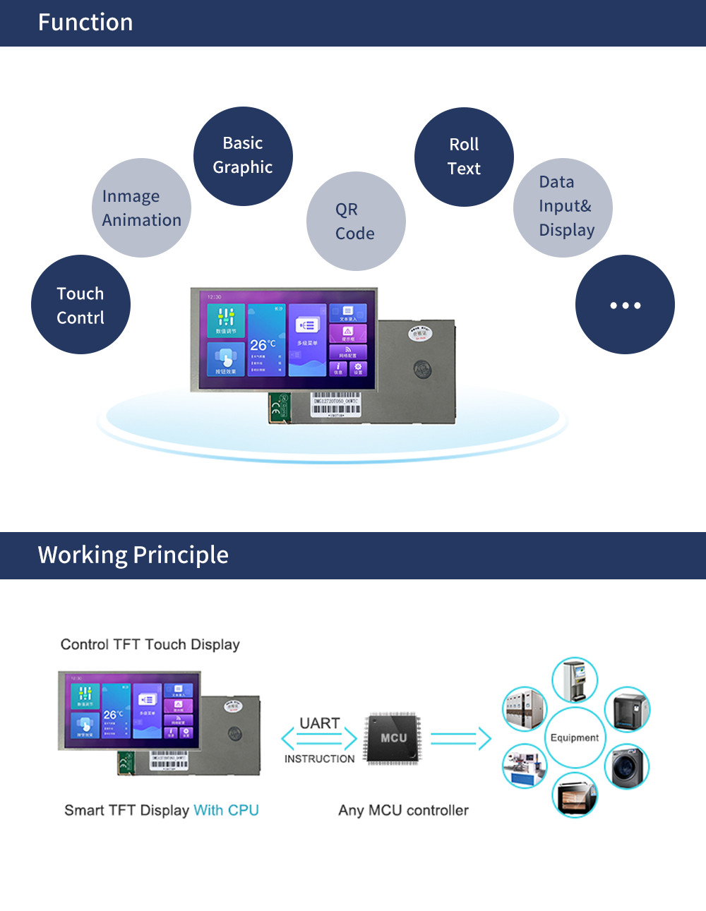
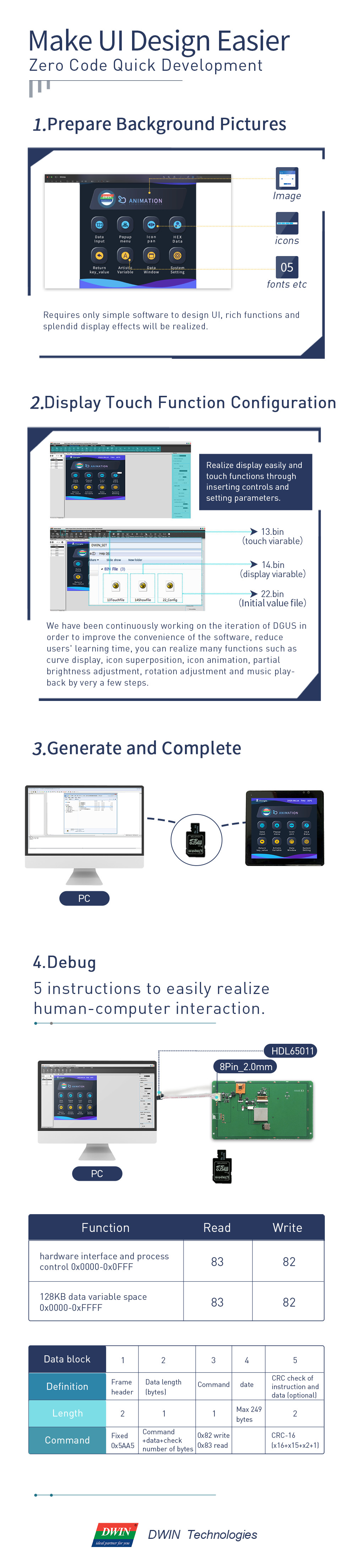
| UI Version | TA / DGUSⅡ (DGUSⅡ pre-installed) | |
| Peripheral | Capacitive touch panel, Buzzer | |
| Dimension | 131.39mm (W) ×83.64mm(H) ×17.75mm(T) | |
| Net Weight | 105g | |
| 1# | 6-36V wide voltage power supply interface | |
| 2# | USB interface, UART1 can be selected | |
| 3# | FLASH expansion module, 3 FLASH modules can be expanded | |
| 4# | 2.54mm through-hole pad, to draw the user resource interface, 20 IO ports, 3 UART serial ports, and 1 CAN port 7 AD ports and 2 PWM ports |
|
| 5# | JTAG interface, connect to HME05 emulator, or connect to PGT05 burner to burn the underlying core firmware. | |
| PIN | Definition | Description |
| 1# | GND | Common ground |
| 2# | RX4 | UART4 Data reception |
| 3# | RX5 | UART5 Data reception |
| 4# | P01 | I / O mouth |
| 5# | CRX | CAN interface data reception |
| 6# | RX2 | UART2 data receiving |
| 7# | P07 | I / O |
| 8# | P15 | I / O |
| 9# | P17 | I / O |
| 10# | P21 | I / O |
| 11# | P23 | I / O |
| 12# | P25 | I / O |
| 13# | P27 | I / O |
| 14# | P31 | I / O |
| 15# | P33 | I / O |
| 16# | FTX | FSK transceiver data reception |
| 17# | ADC0 | AD input |
| 18# | ADC2 | AD input |
| 19# | ADC5 | AD input |
| 20# | ADC7 | AD input |
| 21# | PWM1 | 16bit PWM output |
| 22# | VCC | power input |
| 23# | TX4 | UART4 data transmission |
| 24# | TX5 | UART5 data transmission |
| 25# | P0.0 | I / O |
| 26# | CTX | CAN interface data transmission |
| 27# | TX2 | UART2 data transmission |
| 28# | P06 | I / O |
| 29# | P14 | I / O |
| 30# | P16 | I / O |
| 31# | P20 | I / O |
| 32# | P22 | I / O |
| 33# | P24 | I / O |
| 34# | P26 | I / O |
| 35# | P30 | I / O |
| 36# | P32 | I / O |
| 37# | RST | System reset input |
| 38# | FRX | FSK transceiver data transmission |
| 39# | ADC1 | AD input |
| 40# | ADC3 | AD input |
| 41# | ADC6 | AD input |
| 42# | PWM0 | 16bit PWM output |