Specification
| ASIC Information T5L0 ASIC |
Designed by DWIN. Mass production in 2020, 1MBytes Nor Flash on the chip, 512KBytes used to store the user database. Rewrite cycle: over 100,000 times | |||||
| Color | 262K(262144)colors | |||||
| LCD Type | IPS | |||||
| Viewing Angle | 85/85/85/85 (L/R/U/D) | |||||
| Active Area(A.A) | 49.0mm (W)×73.4mm (H) | |||||
| Resolution | 480X320 | |||||
| Backlight | LED | |||||
| Brightness | EKT035B: 250nit ;100 levels adjustment.(It's not recommend to set brightness to 1%~30% of the maximum, which may lead a flicker) | |||||
| Power Voltage | 6~36V | |||||
| Operation Current | VCC = +12V, Backlight on, 90mA | |||||
| VCC = +12V, Backlight off, 50mA | ||||||
| Working Temperature | -20~70℃(Typical 25℃) | |||||
| Storage Temperature | -30~85℃(Typical 25℃) | |||||
| Working Humidity | 10%~90%RH | |||||
| Baudrate | 3150~3225600bps | |||||
| Output Voltage | Output 1, Iout = 1mA;3.0~3.3 V | |||||
| Output 0, Iout =-1mA;0~0.3 V | ||||||
| Input Voltage (RXD) |
Input 1, Iin = 1mA;2.4~5.0V | |||||
| Input 0, Iin = -1mA;0~0.5V | ||||||
| Socket | 50Pin-0.5mm FCC, | |||||
| SD Card slot | YES (SDHC/FAT32 Format) | |||||
| EKT035B | Capacitive touch panel, Buzzer | |||||
| Dimension | 105.3mm (W) ×119.5mm(H) ×17.6mm(T) | |||||
| Net Weight | 95g | |||||
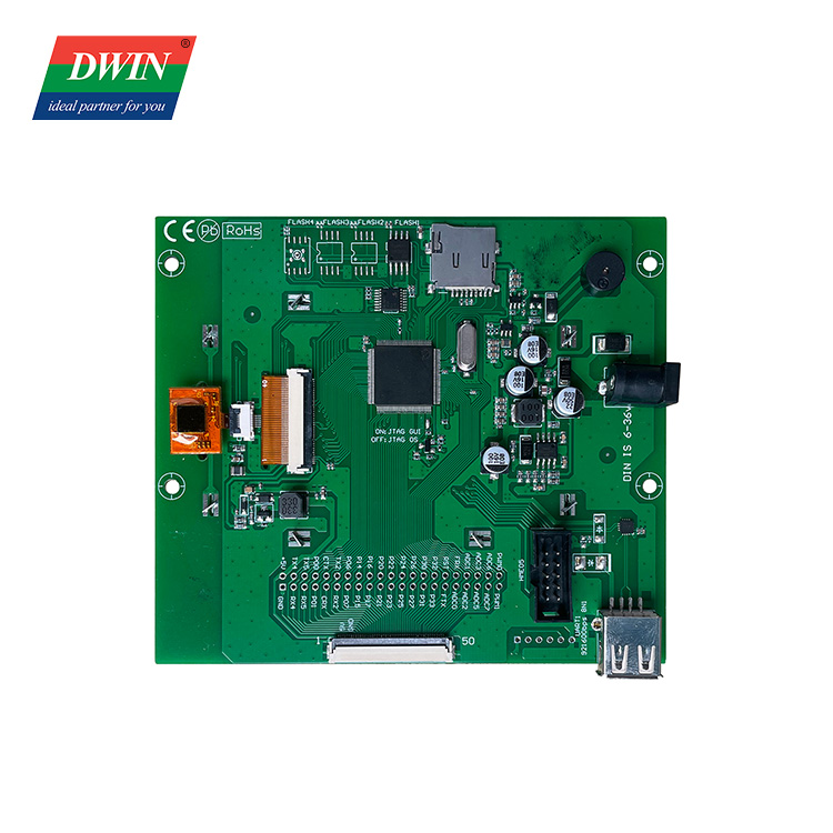
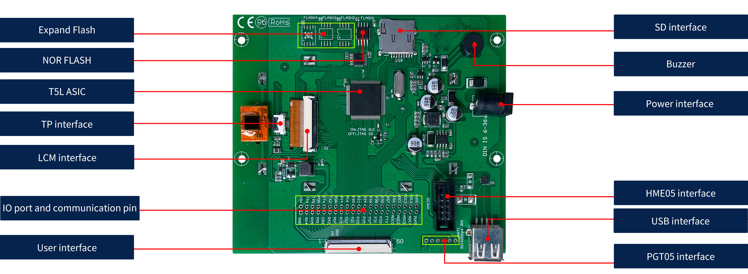
| 1# | The FLASH extension module can be used to expand three FLASH modules | |||||
| 2# | SD card burning interface | |||||
| 3# | Capacitive touch screen interface | |||||
| 4# | LCM interface | |||||
| 5# | 6-36V wide voltage power supply interface | |||||
| 6# | 2.54mm through hole pad GUI / OS CPU outgoing interface | |||||
| 7# | JTAG interface, connected to hme05 emulator or pgt05 burner, used to burn the underlying kernel firmware | |||||
| 8# | USB interface, UART1 can be selected | |||||
| PIN | Definition | Description | ||||
| 1# | GND | Common ground | ||||
| 2# | RX4 | UART4 Data reception | ||||
| 3# | RX5 | UART5 Data reception | ||||
| 4# | P01 | I / O mouth | ||||
| 5# | CRX | CAN interface data reception | ||||
| 6# | RX2 | UART2 data receiving | ||||
| 7# | P07 | I / O | ||||
| 8# | P15 | I / O | ||||
| 9# | P17 | I / O | ||||
| 10# | P21 | I / O | ||||
| 11# | P23 | I / O | ||||
| 12# | P25 | I / O | ||||
| 13# | P27 | I / O | ||||
| 14# | P31 | I / O | ||||
| 15# | P33 | I / O | ||||
| 16# | FTX | FSK transceiver data reception | ||||
| 17# | ADC0 | AD input | ||||
| 18# | ADC2 | AD input | ||||
| 19# | ADC5 | AD input | ||||
| 20# | ADC7 | AD input | ||||
| 21# | PWM1 | 16bit PWM output | ||||
| 22# | 5V | power input | ||||
| 23# | TX4 | UART4 data transmission | ||||
| 24# | TX5 | UART5 data transmission | ||||
| 25# | P0.0 | I / O | ||||
| 26# | CTX | CAN interface data transmission | ||||
| 27# | TX2 | UART2 data transmission | ||||
| 28# | P06 | I / O | ||||
| 29# | P14 | I / O | ||||
| 30# | P16 | I / O | ||||
| 31# | P20 | I / O | ||||
| 32# | P22 | I / O | ||||
| 33# | P24 | I / O | ||||
| 34# | P26 | I / O | ||||
| 35# | P30 | I / O | ||||
| 36# | P32 | I / O | ||||
| 37# | RSTN | System reset input | ||||
| 38# | FRX | FSK transceiver data transmission | ||||
| 39# | ADC1 | AD input | ||||
| 40# | ADC3 | AD input | ||||
| 41# | ADC6 | AD input | ||||
| 42# | PWM0 | 16bit PWM output | ||||

DMG80480F070_01W (COF Series)